

研究内容
RESEARCH
機能性材料研究開発
Development of
a functional material
CLBO
機能性材料研究開発
Development of
a functional material
GaN
結晶の多形制御
Polymorphism in crystals
機能性材料研究開発
Development of a functional material
GaN
情報・低炭素社会における
マテリアルイノベーション
Materials innovation in information-technology (IT) and low-carbon societies
情報化社会で一般化するIoTで必須となる5Gや低炭素社会に不可欠なマテリアルイノベーションとして、 青色発光ダイオードで脚光を浴びた窒化ガリウムGaN結晶の高品質結晶化技術の創出があります。 当研究室では「Naフラックス法」や「OVPE法」という全く新しいGaN結晶の育成方法を発見・開発し、 世界で最も高品質なGaN結晶育成に成功しています。このような新しい結晶育成技術の実用化を目指し、 環境省の省エネプロジェクト、文部科学省のGaN拠点プログラムをはじめ他大学や10社を越える様々な 企業との共同研究によって推進しています。
One of the essential material innovations for low-carbon society and 5G, which is crucial for the IoT generalized in the information society, is the creation of high-quality crystallization technology for gallium nitride GaN crystals, which has been highlighted as an application for blue light emitting diodes. In our laboratory, we have discovered and developed completely new GaN crystal growth methods such as "Na-flux method" and "OVPE method", and succeeded in growing the highest quality GaN crystal in the world. Aiming to put these new crystal growth technologies into practical use, we are promoting them through collaborative research with other universities and more than 10 companies, including the Ministry of the Environment's energy conservation projects and the Ministry of Education, Culture, Sports, Science and Technology's GaN base program.
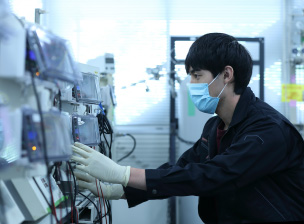
Naフラックス法大型炉によるGaN育成の様子
GaN growth in a large furnace by Na-flux method.
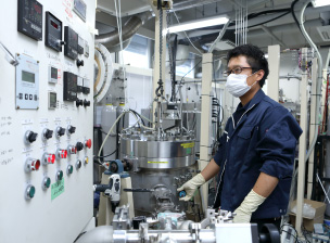
OVPE成長装置1200℃以上の高温で育成します
OVPE growth equipment. Grown at a high temperature higher than 1200℃.
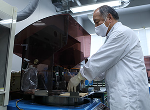
GaN結晶研磨の様子
GaN crystal polyshing process.
